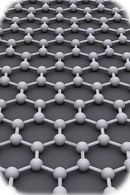

Good materials characterization is required across all steps in the creation of new graphene devices -- from guiding the initial graphene synthesis, transfer to the desired substrate, and understanding chemical modification and analysis of the finished device. Our webinar presentation shows how a multi-technique approach using both Raman spectroscopy and XPS can address the challenges posed at these steps.
Raman microscopy is well suited for the characterization of graphene. A vibrational spectroscopy, it is very sensitive to small changes in the geometric structure of a molecule and its environment. This sensitivity makes Raman an ideal probe for a number of important properties specific to graphene and nanotube samples, such as layer thickness, sample integrity and tube diameter.
X-ray photoelectron spectroscopy (XPS) is ideally suited to the determination of the surface chemistry and the way in which that chemistry changes in the surface and near-surface region. The technique provides quantitative elemental and chemical information with extremely high surface specificity and is ideal for comprehensively and quantitatively characterizing the elemental composition and chemical bonding states in graphene and carbon nanotubes.
Using both techniques in concert allows analysts to completely characterize carbon nanomaterials. Our webinar demonstrates the utility of these techniques, illustrated by examples from graphene samples created by mechanical exfoliation, chemical reduction and CVD methods.
Areas of Interest – Graphene Devices
- Transparent conductive electrode for microelectronics
- Thin film transistors
- Touch Screen Devices
- Graphene-based catalytic systems
- Molecular Sensors.
Date:
Thursday, March 21, 2013
Time:
Session 1 - 3 p.m. CET / 10 a.m. EDT / 14:00 GMT
Session 2 - 4 p.m. EDT / 3 p.m. CDT / 1 p.m. PDT / 20:00 GMT
Duration:
1 hour
